The pull-down menu described earlier is mainly used for administrative tasks, such as loading and saving circuit descriptions and GUI configuration settings. The actual creation of circuit elements is carried out with the help of the toolbar, from which the user selects logic gates to place on the workarea and operations to modify the circuit. Unlike the pull-down menu, the toolbar is accessible using the mouse only and not the keyboard.
The toolbar is comprised of a vertical column of iconic buttons along the side of the main window. The user may configure the GUI so as to have the toolbar displayed on either the left or right side of the main window. The toolbar provides three major operations, hence the partitioning of the toolbar into three main blocks.
The first block of operations relates to Component creation. Using these buttons, the user can quickly create and place logic gates on the workarea. Currently, the software supports the creation of AND, NAND, OR, NOR, XOR, XNOR, BUFFER and NOT gates. These gates are hardcoded in the current implementation of the script. However, future versions may consult a library upon initialization, during which the circuit editor will be informed of all the gates and components supported by the underlying simulator engine. These gates and components can then be presented to the user by the GUI.
After single-clicking the appropriate toolbar button with the mouse, the user moves the mouse pointer onto the canvas; the new logic gate will be created and will follow the mouse as it is dragged across the canvas. The user can place the component by clicking the leftmost mouse button at the desired location on the workarea. The gate may also be rotated before placement by clicking the middle mouse button; hitting the rightmost mouse button cancels the placement and removes the gate from the canvas. More details on the implementation of component creation is presented in Section 3.5.1.
The second block of buttons contains the Edit
operations. Using these features, the user can move and delete circuit
elements, rotate components, and modify various attributes of the
circuit elements. These operations all behave in a similar manner, with
the leftmost mouse button carrying out the operation on the selected
circuit element and the rightmost mouse button terminating the
operation. In the case of component rotation, the leftmost and middle mouse
buttons rotate the target component ![]() counter-clockwise and
counter-clockwise and
![]() clockwise, respectively. Any wires connected to the
component are moved accordingly. This is accomplished by subjecting
each of the wire points connected to the ports of the component
to the same rotation matrix used to rotate the component itself.
clockwise, respectively. Any wires connected to the
component are moved accordingly. This is accomplished by subjecting
each of the wire points connected to the ports of the component
to the same rotation matrix used to rotate the component itself.
The GLUE button on the Edit section lets the user glue several circuit items together by holding down the leftmost mouse button on the canvas and stroking out a bounding box with the mouse. All circuit elements which lie inside the box after the mouse button is released will be treated as a single entity. This makes it easier to perform an operation on several circuit items simultaneously. For example, several gates and wires could be glued together and then subsequently moved as a single unit. This makes manipulation of the circuit much easier than moving each of the elements individually. The unglue operation will remove the bounding box, thus enabling the user to once again manipulate the circuit elements as separate units.
The last block of buttons in the toolbar contains the Wire creation and manipulation operations. Using these buttons, the user can create, identify, label and solder netlists, which are responsible for connecting components and propagating signals.
The CREATE button changes the mouse pointer to a wire spool which is used to layout netlists on the workarea. The leftmost mouse button is used to lay down each of the wire points and the middle mouse button completes the wire. The rightmost mouse button aborts the netlist creation operation and removes all the points just created. During wire creation, rubber-banding of the wires is used so as to provide the user with immediate feedback of how the current wire will be placed. The user may configure the interface so that only vertical and horizontal (manhattan style) wires may be drawn. In addition, if the user sets a wire point on top of an existing wire, an existing wire point or a port, the new point will automatically be soldered to that item. These features may be enabled or disabled using the configuration dialog box described in Section 2.4.
The SOLDER button lets the user solder two netlists together
or solder a netlist to the port of a component. After pressing this button,
the mouse pointer will change into a soldering iron on the workarea.
Clicking the leftmost mouse button on top of wires, wire points and
ports will solder all the overlapping items together. All the items
under the cursor will be soldered intelligently -- the
soldering feature prevents the creation of cycles in a netlist and
prohibits the soldering of two output netlists together.![]() The soldering feature can also be used to introduce wire points along an
existing wire. One important feature currently lacking in the circuit
editor is the ability to ``unsolder'' wires. However, the
same end result can be achieved by introducing a new wire point next
to the soldering point and then deleting the intervening wire segment.
The soldering feature can also be used to introduce wire points along an
existing wire. One important feature currently lacking in the circuit
editor is the ability to ``unsolder'' wires. However, the
same end result can be achieved by introducing a new wire point next
to the soldering point and then deleting the intervening wire segment.
Once netlists have been created and soldered together, the NETLIST button can be used to identify netlists. After clicking this button and moving the mouse pointer to a netlist element (that is, a wire or wire point) on the workarea, all wires and points which comprise the corresponding netlist will be highlighted. This feature can be used to verify the connectivity of the circuit since the inter-connections of the circuit may not be immediately obvious based upon visual inspection alone. Note that netlist extraction is not done each time the button is pressed. Instead, we rely upon the dynamic netlist identification feature to identify and tag netlist items as wires and points are laid down and soldered. This is described more fully in Section 3.6.1.
Finally, the LABEL button can be used to name the netlists for both documentation and simulation purposes. After pressing this toolbar button, the user moves the mouse pointer to a wire point in the netlist that is to be named and clicks the leftmost mouse button. A dialog window, as shown in Figure 2.3, is displayed which lets the user supply a netlist name and specify the orientation of the label with respect to the point. After providing a name and orientation, the user presses the OK button, and a waveform corresponding to the label is created in the signal display window, which is described in Section 2.3.2.
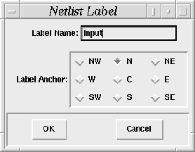
Figure 2.3: Netlist Label Dialog Box
Note that only wire points and not the wires themselves can be labelled. Also, the interface prohibits the user giving two netlists the same name or a single netlist two names. As a consequence, the user cannot solder together two netlists which have already been labelled. The name and orientation of labels may be changed using the MODIFY button of the Edit section of the toolbar. Labels may also be deleted using the DELETE button of the toolbar. After the deletion of the label, the corresponding waveform in the signal display window will also be removed.