We first start with a trace of a simple combinational circuit, a three-input AND gate. The initial configuration of the circuit and the external wires is shown in Figure A.1. Recall that the Wire constructor places an X as the initial signal of all wires.
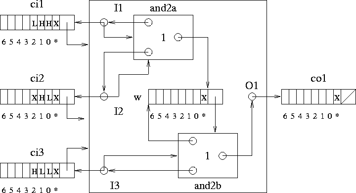
Figure A.1: Three-Input AND Gate Before Simulation
When the three-input AND gate receives the simulate() message, the first thing the component does is to determine if all of its inputs are ready. Since the component is at time `*' and because all wires initially have an unknown stored at that initial time, the algorithm enters the body of the while loop and increments the local time of the component. Hence the local time of the three-input AND gate is now zero. The component then sends the is_lowest_level() message to its input port list to determine if the component does not have any nested subcomponents. In this case, the three-input AND gate does have subcomponents, so the descend() message is sent to the input ports list. This method will start scanning all the input ports, sending simulate() messages to all the components which are directly connected to the inputs.
It will be assumed that the first subcomponent to receive the simulate() message is the and2a gate. As with the three-input AND gate, this component now determines if all of its inputs are ready. Obviously, they are, so the local time of the and2a gate is increased to zero and the is_lowest_level() message is sent to its input ports to determine if the component does not have any subcomponents. This is now the case, so its virtual process() function is executed after the delay time is validated. The process() message reads the X signals from the wires ci1 and ci2 at time `*' and performs a logical AND operation on them producing another unknown X at time zero. This signal is then sent and stored in the nested wire in the three-input AND gate. The wire then takes control and sends simulate() messages to all the components to which it is connected. The only component in the wire's fan-out is the and2b gate.
Now the inputs to the and2b gate are ready, so its local time is incremented to zero and its initial unknown inputs are read from the nested wire and the ci3 wire by the process() method. The resulting signal, X, is sent to the output wire co1 at time t = 0. Since this wire has no fan-out, any attempt it makes to propagate its signals is immediately rejected. Control returns back to the and2b gate, where it determines that it still has inputs waiting to be processed. Its local time increases to one and its virtual process() method is invoked. The X input of the nested wire and the L input of the ci3 wire is read and an L signal is sent to the output wire at time t = 1. When control is returned back to the and2b gate, it realizes that all of its inputs are gone, and control eventually returns back to and2a.
Since and2a has inputs ready at time t = 0, its local time is incremented to one and the H and the L signals are read from ci1 and ci2 respectively. The resulting L signal is sent to the nested wire at time t = 1. The wire once again passes control to the and2b gate which increments its local time to two and reads the two L signals from its input wires. It sends an L signal to the output wire which returns control back to the and2b gate. Upon realizing that all its inputs have once again been consumed, control returns yet again to the and2a gate.
The and2a gate determines that it has two signals waiting for it at time t = 1 and therefore increments its local time to two. The two H signals are read from the wire and processed with the resulting H signal being sent to the nested wire at time t = 2. The wire passes control to and2b which increments its local time to three and processes the two H signals from ci3 and the nested wire. It then sends the resulting H signal to the output wire at time t = 3. Control is returned back to and2a since and2b can go no further.
After incrementing its local time to three, the and2a gate reads the final L and X signals from its two input wires and sends the resulting L to the nested wire. When this wire passes control to the and2b gate, and2b notices that it has a signal L waiting for it on the nested wire at time t = 3, but there is no corresponding signal on ci3. Therefore, control is eventually returned back to and2a which realizes that it too has consumed all of its inputs.
Control is finally passed back to the encompassing three-input AND gate. This component continues to trivially execute its outer while loop, incrementing its local time through each iteration. Every time it tries to send a message to its subcomponents, telling them to simulate, control is immediately returned back since all of its subcomponents are finished. Eventually, the local time of the three-input AND gate reaches three, and it realizes that all of its inputs have been processed, hence terminating the simulation. The final configuration of the internal and external wires after the simulation is shown in Figure A.2.
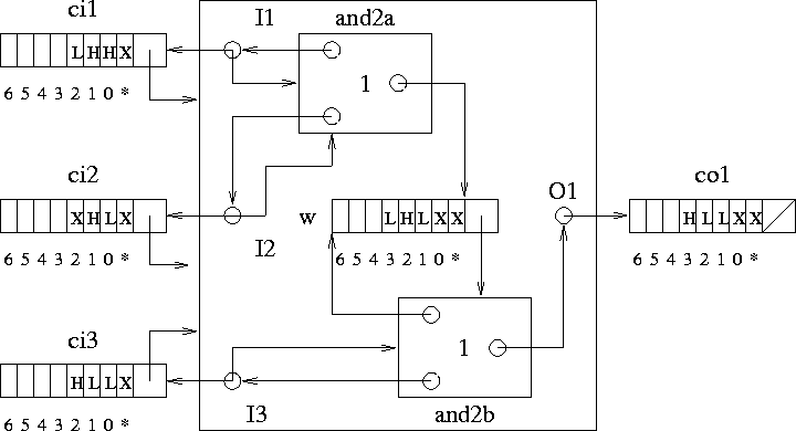
Figure A.2: Three-Input AND Gate After Simulation