As mentioned earlier, an enhancement mode MOSFET can be modeled as a simple switch, through which current can flow in either direction. A slightly more complex model could be to consider the device to act as a resistor on its output, and a capacitor at its input. More sophisticated models can be readily derived, but the two mentioned above are useful for logic and approximate timing simulations of the behavior of a MOS integrated circuit.
A number of circuit simulation programs have been written which allow the simulation of MOS integrated circuits with a wide range of transistor models. Some of the more sophisticated models have many parameters which can be varied, and can produce quite accurate simulation results. Most of these circuit simulators have been derived from the SPICE circuit simulation program, developed at UCB. SPICE has 3 sophisticated models for MOS transistors, and is generally considered to be quite an accurate circuit simulator.
We can derive the simplest (and least accurate) of the SPICE models from simple physics; this exercise is useful because it provides some ``rules of thumb'' for the design of VLSI devices. In particular, it allows us to see how devices ``scale''; that is, how important properties such as the switching speed of a transistor vary with the linear dimensions of the transistor.
One of the most important parameters for a transistor is its ``switching
time''. We might expect this to be related to the transit time,  , for
a charge carrier (an electron, for an N channel MOSFET or a hole, for a P
channel MOSFET) to cross the
channel region from the source to the drain region
, for
a charge carrier (an electron, for an N channel MOSFET or a hole, for a P
channel MOSFET) to cross the
channel region from the source to the drain region![]() .
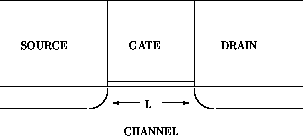
If we consider a transistor as shown in
Figure
.
If we consider a transistor as shown in
Figure ![]() ,
the transit time,
,
the transit time,
 , is simply
  where v is the average speed of the
charge carrier.
where v is the average speed of the
charge carrier.
Under simple conditions, we can calculate the average speed, v, for a
charge carrier. If no nuclei were present in the channel region, and there
was no voltage applied between the source and the drain ( i.e., no applied
electric field) across the channel, then the average velocity would be
zero. If there was an electric field in the channel region, the charge
carriers would accelerate with an acceleration  , where e is the
charge of the charge carrier, E is the magnitude of the applied electric
field, and m is the mass of the charge carrier.
(The quantity e is equal in magnitude to the charge of an electron).
For free charge carriers, the average speed would be
, where e is the
charge of the charge carrier, E is the magnitude of the applied electric
field, and m is the mass of the charge carrier.
(The quantity e is equal in magnitude to the charge of an electron).
For free charge carriers, the average speed would be  ,
where t is the time for the charge carrier to travel across the
channel region. In reality, however, the charge carriers will collide with
the nuclei in the channel region quite frequently. This collision is
inelastic, the charge carrier gives up some of its energy to the nucleus.
We will assume that the collisions are totally inelastic, and that each
collision brings the charge carrier to a stop. The
electron, therefore, accelerates only in the interval between collisions
with nuclei. There will be an ``average time between collisions'',
,
where t is the time for the charge carrier to travel across the
channel region. In reality, however, the charge carriers will collide with
the nuclei in the channel region quite frequently. This collision is
inelastic, the charge carrier gives up some of its energy to the nucleus.
We will assume that the collisions are totally inelastic, and that each
collision brings the charge carrier to a stop. The
electron, therefore, accelerates only in the interval between collisions
with nuclei. There will be an ``average time between collisions'',
 , and the average speed of the charge carrier will be given by
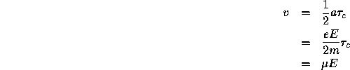
The parameter  is called the ``mobility''; there is an
``electron mobility'',
is called the ``mobility''; there is an
``electron mobility'',  , and a corresponding
``hole mobility``,
, and a corresponding
``hole mobility``,  .
For silicon,
.
For silicon, 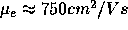 and,
and, 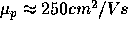 .
(Actually, there are two types of mobility; a ``bulk'' mobility and a
``surface'' mobility. For MOSFET's, the surface mobility is important,
and corresponds to the values quoted. For bipolar transistors, the bulk
mobility is important.)
.
(Actually, there are two types of mobility; a ``bulk'' mobility and a
``surface'' mobility. For MOSFET's, the surface mobility is important,
and corresponds to the values quoted. For bipolar transistors, the bulk
mobility is important.)
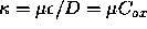
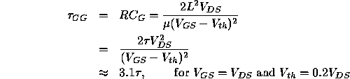
So, the characteristic time,  , for the transistor is
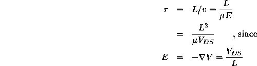
Although this is not a rigorous derivation, there are two important things to note:
 is proportional to the square of the
channel length.
is proportional to the square of the
channel length.
 is inversely proportional to
  .
.
These are ``scaling rules'' for MOS devices, and are believed to be approximately valid for device sizes (channel dimensions) down to about 0.5 microns.
We can also calculate, approximately, some of the important electrical
properties of the MOS transistor; e.g., the current which can flow through
the channel region, and the impedance of the channel. These will be
functions of both the size of the channel region and of the voltages
applied to the gate ( ), drain (
 ) and source (
 )
of the device.
)
of the device.
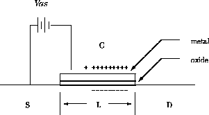
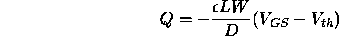
Referring to
Figure ![]() ,
the charge, Q, which will be available at the
oxide/channel boundary is simply
,
the charge, Q, which will be available at the
oxide/channel boundary is simply 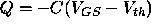 where C is the capacitance of the capacitor formed between the gate and the
substrate,
where C is the capacitance of the capacitor formed between the gate and the
substrate,  is the gate-to-source voltage, and
  is the
threshold voltage. (The quantity
is the
threshold voltage. (The quantity  is the
``effective'' voltage applied to the gate).
For a parallel plate capacitor,
is the
``effective'' voltage applied to the gate).
For a parallel plate capacitor,  where A = LW is the
area of the gate over the channel of width W and length L, D is the
distance between the gate and the substrate ( i.e., the oxide thickness) and
where A = LW is the
area of the gate over the channel of width W and length L, D is the
distance between the gate and the substrate ( i.e., the oxide thickness) and
 is the permittivity of the material
(for
is the permittivity of the material
(for 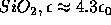 .) So,
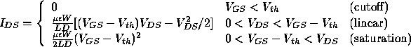
The current flowing in the channel is
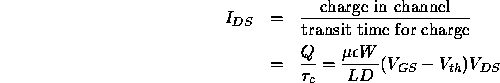
(Note that this analysis neglects some important effects; for example, it implicitly assumes that there is a uniform electric field in the entire channel region.) A more sophisticated analysis gives slightly different values for the current in the channel region:

in the linear (ohmic) region, and
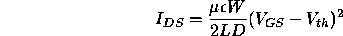
in the saturation region.
These expressions are often written in terms of the ``process transconductance
parameter'',  , where
 where
where  is
the capacitance per unit area of the oxide. The gate capacitance
is
the capacitance per unit area of the oxide. The gate capacitance
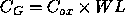 . The quantity
  is a SPICE
parameter for MOS transistors.
is a SPICE
parameter for MOS transistors.
We can now calculate the effective impedance of the channel region as:
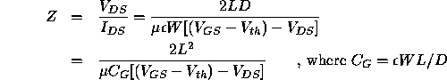
if the transistor is operated in the linear region, and
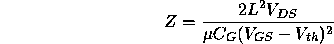
in the saturation region.
The fact that the impedance, Z, for a MOS transistor is proportional to the
ratio  in both their linear and saturated regions means that we can
use these transistors as resistors; the relative resistances
scale with the device size. This is true for both P- and N- channel
devices, as well as for both enhancement and depletion mode transistors.
In fact, a ``permanently turned on'' transistor is often used as a
resistor, for example as a ``pull-up resistor'' for a logic gate, to
provide a current limit for the gate output.
in both their linear and saturated regions means that we can
use these transistors as resistors; the relative resistances
scale with the device size. This is true for both P- and N- channel
devices, as well as for both enhancement and depletion mode transistors.
In fact, a ``permanently turned on'' transistor is often used as a
resistor, for example as a ``pull-up resistor'' for a logic gate, to
provide a current limit for the gate output.
We can also calculate the time constant  for a transistor
to charge the gate of another identical transistor. This time is very
important, since it will be related to the ``gate delay'' for a logic
device.
for a transistor
to charge the gate of another identical transistor. This time is very
important, since it will be related to the ``gate delay'' for a logic
device.
assuming that the transistor providing the charge is operating in its
saturation region. Although this result is not rigorously correct, it is
worth noting that the delay time for a transistor to switch on a second
transistor has a simple relationship to the transit time  .
.
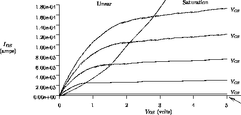
Figure ![]() shows a plot of the current in the channel region of a MOS
transistor
shows a plot of the current in the channel region of a MOS
transistor  , the current between the source and drain) against
the potential difference across the channel
, the current between the source and drain) against
the potential difference across the channel  for various
values of the applied gate current,
for various
values of the applied gate current,  for a typical MOS
transistor
for a typical MOS
transistor![]() .
.
Note that three different regions are distinguished; the ``cutoff'' region, in which the transistor effectively passes no current; the ``linear'' region, in which the behavior is ohmic, and the ``saturation'' region, in which the current is nearly constant.
Effectively, then, we have modelled the current in the channel region of a MOS transistor (either enhancement mode or depletion mode, P- or N- channel) as
The quantity  is often written as
  , and is
called the ``gain factor'' for a MOS transistor. Note that
, and is
called the ``gain factor'' for a MOS transistor. Note that  is
proportional to
is
proportional to  .
.
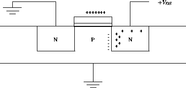
Actually, in the saturation region, the drain current,  is not
completely independent of
is not
completely independent of  , partly because
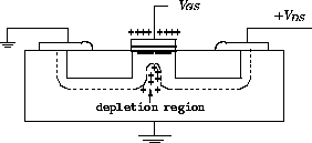
  ``depletes'' charge carriers from the vicinity of the well as shown in
Figure
``depletes'' charge carriers from the vicinity of the well as shown in
Figure ![]() .
This effect both shortens the effective channel length and adds
more charge carriers to the channel region.
.
This effect both shortens the effective channel length and adds
more charge carriers to the channel region.
These effects, which increase the drain current  are
usually modelled empirically by the parameter
are
usually modelled empirically by the parameter  , the ``channel
length modulation factor'', giving the following expression for the
saturation current
, the ``channel
length modulation factor'', giving the following expression for the
saturation current

 is typically quite small,
  .
It is a Level 1 SPICE parameter. The term
.
It is a Level 1 SPICE parameter. The term  is
often included with the expression for
is
often included with the expression for  in the linear region as
well, to ensure that
in the linear region as
well, to ensure that  is continuous from the linear to the
saturation region.
is continuous from the linear to the
saturation region.
One remaining parameter for MOS devices which can readily be derived using
simple physical reasoning is  , the threshold voltage
![]() .
.
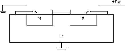
We start by looking again at a schematic of the cross-section of an NMOS
enhancement mode transistor, as in
Figure ![]() (similar arguments apply for a PMOS transistor.)
(similar arguments apply for a PMOS transistor.)
Note that if no charge is applied to the gate, the source and drain regions are separated by reverse biased PN junctions, and no current can flow between the source and drain of the transistor. (The ``off'' impedance is normally of the order of thousands of megohms.)
When a positive charge is applied to the gate of the transistor, however,
mobile charge carriers are attracted from the bulk of the P-doped
substrate to the surface of the channel region immediately below the
insulating oxide under the gate. These mobile charge carriers leave behind
fixed (immobile) charges in the ``depletion'' region in the channel, as
shown in
Figure ![]() .
The thickness,
.
The thickness,  of the depletion region below the gate can be
calculated as a function of
of the depletion region below the gate can be
calculated as a function of  , the electrostatic potential just
inside the depletion layer at the oxide-semiconductor interface. In P-type
semiconductors, this depletion layer is made by ``pushing back'' mobile
holes.
, the electrostatic potential just
inside the depletion layer at the oxide-semiconductor interface. In P-type
semiconductors, this depletion layer is made by ``pushing back'' mobile
holes.
The number of holes, dQ, originally contained in a thin horizontal layer of
thickness  is
is

The change in surface potential  is
is
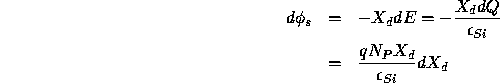
integrating,
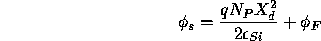
where  is the constant of integration. Solving for
  ,
,
where  is the permittivity of silicon, q is the charge of a
single charge carrier (|q| = e, the charge of an electron), and
is the permittivity of silicon, q is the charge of a
single charge carrier (|q| = e, the charge of an electron), and  is the density of P-type ions in the substrate.
The quantity of charge per unit area in the channel region due to the immobile ions which have been stripped of their charge carriers (in this case, ions which have been stripped of their mobile holes) is

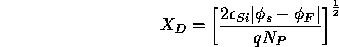
The threshold is defined as  , i.e., the induced
surface potential is equal in magnitude to the original, unbiased surface
potential; the density of mobile negative charge carriers (electrons)
at the surface is equal to the density of holes in the original, unbiased
substrate. In effect, the channel region has been ``induced'' to become
as strongly N-doped as it was originally P-doped.
, i.e., the induced
surface potential is equal in magnitude to the original, unbiased surface
potential; the density of mobile negative charge carriers (electrons)
at the surface is equal to the density of holes in the original, unbiased
substrate. In effect, the channel region has been ``induced'' to become
as strongly N-doped as it was originally P-doped.
In order to calculate the gate voltage  required to attain
threshold, we need to know the concentration of charge carriers N in the
unbiased substrate. This is normally equal to the dopant concentration of
the substrate.
required to attain
threshold, we need to know the concentration of charge carriers N in the
unbiased substrate. This is normally equal to the dopant concentration of
the substrate.
We can define the equilibrium (electrostatic) potential  inside a
semiconductor as
inside a
semiconductor as
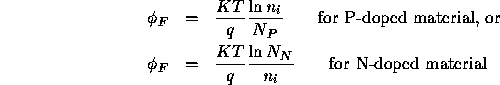
where  or
or  are the equilibrium concentrations of
P or N type mobile charge carriers ( i.e. the dopant concentration) in
the substrate, and
are the equilibrium concentrations of
P or N type mobile charge carriers ( i.e. the dopant concentration) in
the substrate, and  is the equilibrium mobile charge concentration
for pure (or ``intrinsic'') silicon,
is the equilibrium mobile charge concentration
for pure (or ``intrinsic'') silicon, 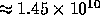 at
room temperature. Note that the potential
at
room temperature. Note that the potential  is a surface
potential, possibly arising from the diffusion of charge carriers across a
surface. This potential is, of course, present independent of the gate
voltage
is a surface
potential, possibly arising from the diffusion of charge carriers across a
surface. This potential is, of course, present independent of the gate
voltage  . Moreover, it must be ``overcome'' by
  to
allow conduction in the channel.
to
allow conduction in the channel.
If the substrate is not biased by any ``substrate body bias''
 then the immobile charge in the depletion region at
threshold
then the immobile charge in the depletion region at
threshold  is
is

If the substrate is biased by a voltage  between the source and
body, the surface potential required to produce inversion is
between the source and
body, the surface potential required to produce inversion is
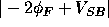 , and
, and

We can now calculate the gate voltage required to produce inversion,
the threshold voltage  . The threshold voltage consists of several
components:
. The threshold voltage consists of several
components:
 , to change the surface
potential and offset the immobile depletion layer charge
, to change the surface
potential and offset the immobile depletion layer charge  .
.
 is the capacitance per unit area of the gate oxide;

 .
For silicon gate devices,
.
For silicon gate devices,  .
.
 .
.
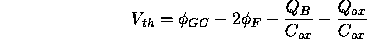
Therefore the threshold voltage  is given by
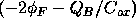
Since the last term in the previous expression is difficult to evaluate it is usual to express the threshold voltage as a function of the substrate bias voltage, and measure the unbiased threshold voltage:
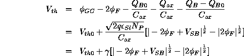
where
 .
The parameter
.
The parameter  is the zero bias threshold voltage and
  is called the ``body effect coefficient factor''.
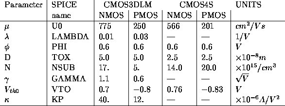
We have now derived the most important relationships used in the simplest of the SPICE models (Level 1) of the MOS transistor. The following table lists estimates of these parameters for the CMOS3DLM and CMOS4S processes available to us:
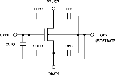
Circuit simulators include the capacitance between the various
elements of the transistor as components of the models.
SPICE calculates the nonlinear capacitance![]() between the gate and channel region.
SPICE uses a set of parasitic capacitances modeled as constant capacitors
as shown in
Figure
between the gate and channel region.
SPICE uses a set of parasitic capacitances modeled as constant capacitors
as shown in
Figure ![]() ,
in which the parasitic
capacitors are named as in the SPICE parameter list. Also shown are the
capacitances between the source and body, and the drain and body.
These are each considered as two separate nonlinear capacitors, a bottom
capacitance and a sidewall capacitance, calculated from
the perimeters of the source and drain areas.
,
in which the parasitic
capacitors are named as in the SPICE parameter list. Also shown are the
capacitances between the source and body, and the drain and body.
These are each considered as two separate nonlinear capacitors, a bottom
capacitance and a sidewall capacitance, calculated from
the perimeters of the source and drain areas.